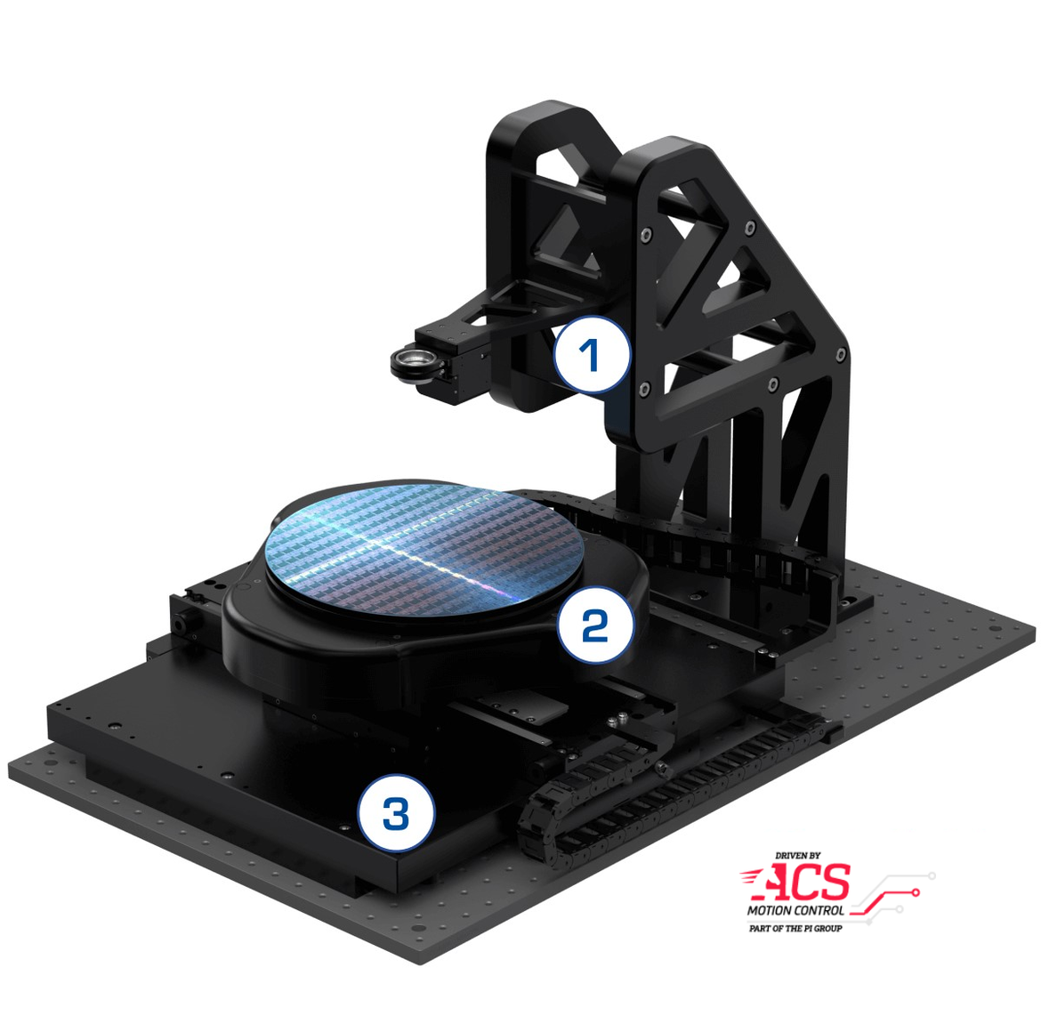
Wafer Stealth Dicing
Motion Solutions Enabling Chip Singulation with High Throughput and Precision
In the production of (micro)chips, it is necessary to separate the individual dies from the wafer. Stealth laser dicing involves creating a modified layer within the wafer by focusing a laser below the surface, then using a tape expander to separate the chips. Typical challenges faced are contamination risks to the wafer, accurately positioning the modified layer onto both XY axes to enable the narrowest possible streets, and maintaining the focus within the wafer and track wafer distortions. At the same time, the highest possible scanning speed is necessary to ensure high throughput. As requirements continue to increase, stealth laser dicing is becoming the first choice for high-volume, MEMS dicing, or smaller and more complex dies. PI responds to the demands of laser-dicing processes with motion systems offering both high accuracy and a high level of straightness at high velocities.
Z Axis - High-Dynamic Laser Focus Control
- Wear-free, lever-amplified piezo drives for 24/7 operations without particle generation
- Mechanical design with high stiffness and high resonant frequencies for high dynamics and short settling times and for high payload of larger objectives
- Up to 800 μm travel range to match the wafer thickness
- Fine positioning with subnanometer resolution
>> P-725 PIFOC® Objective Scanner
θX/θY/Z Axis - High-Precision Wafer Alignment and Positioning
- Parallel-kinematic design for wafer adjustment and offset corrections in three dimensions
- Direct drive linear motor with air bearings for high-precision levelling
- Frictionless design with minimal hysteresis provides high repeatability and adjustments in the nanometer range
- Low-profile design for easy integration
- Maintenance-free with long lifetime in 24/7 operations
>> A-523 Z Tip/Tilt Stage
XY Axis - High-Dynamic Wafer Scanning Motion
- Air bearing planar system featuring ironless linear motors for fast step-and-settle
- No wear, no tear design ideal for 24/7 high duty cycle operation
- Minimal runout errors and nanometer straightness and flatness
- Low profile, monolithic design allows easy integration to system level solutions
>> A-311 Air Bearing Planar Scanner
Advanced Automation Control
- EtherCAT® motion control and drive modules provide open network connectivity
>> Controller & Drives - Laser control module enables accurate synchronized trigger of laser based on motion profile
>> Laser Control Interface - Advanced algorithms like ServoBoost™ provide fast step-and-settle and exceptional constant scanning velocity
>> ServoBoost™ - NanoPWM™ drive technology optimizes velocity and enables accurate tracking
>> NanoPWM™ Drives - Integrated piezo axes deliver synchronized height control
>> Motion Controller
System in Motion


