The mainstreaming of photonics - the science and application of light waves - keeps accelerating. Pandemic-driven data-consumption has hastened adoption of silicon photonics (SiPh) to enable new capacity, architectural flexibility, and energy-efficiency for data centers. Unlike the telephony-driven demand that fueled the first photonic boom in 1997-2002, today’s exponentiating broadband requirements are propelled by many disparate applications, from streaming media to social networks, personal medicine, genomics, and of course, the dreaded teleconferencing that sustained business and personal relationships throughout a difficult 2020.
Soon, the world will be girdled by constellations of tens of thousands of low-orbit satellites using laser beams to transfer data around the planet and between each other to provide low-latency Internet access, all in service of mankind’s insatiable and growing appetite for data. More of a surprise is the sudden implementation of photonic technologies in consumer and business applications such as photonic cables that offer conveniently long lengths while keeping pace with the latest high-speed, optical interface technologies (http://www.oeic.vn/capabilities.htm#auto-optical-alignment) and even bio-sensors built into wearables, such as the blood pressure/hydration/glucose sensors conjectured for coming generations of the Apple Watch (https://gadgetsandwearables.com/2021/05/02/rockley-apple-hydration/).
The blossoming possibilities of a photonics-enabled future mirrors the Silicon Revolution of the late 1970s and early 1980s, when marvels like pocket calculators (https://en.wikipedia.org/wiki/HP-19C/-29C) and personal computers (https://en.wikipedia.org/wiki/Apple_II) first found a place in businesses and homes. Then, as now, the challenge was scaling manufacturing to keep pace with demand, competitive pressures, and relentless technological advancements.
In the early days of semiconductor manufacturing, the thriving ecosystem of toolmakers that we take for granted today did not exist. Today, you can build a new fab from the ground up just by issuing purchase orders, but take a look at historical video from the dawn of the Silicon Revolution (https://www.chiphistory.org/128-an-intel-wafer-fab-cleanroom-circa-1980) and you cannot help but be impressed by the labor-intensive processes and custom-built machinery at the industry's birth.
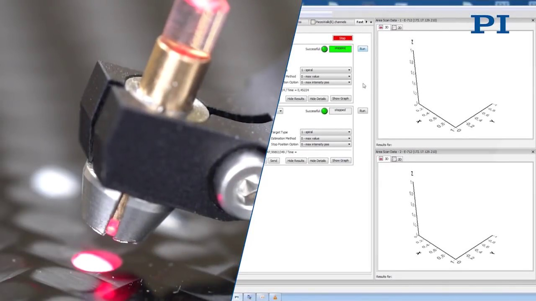
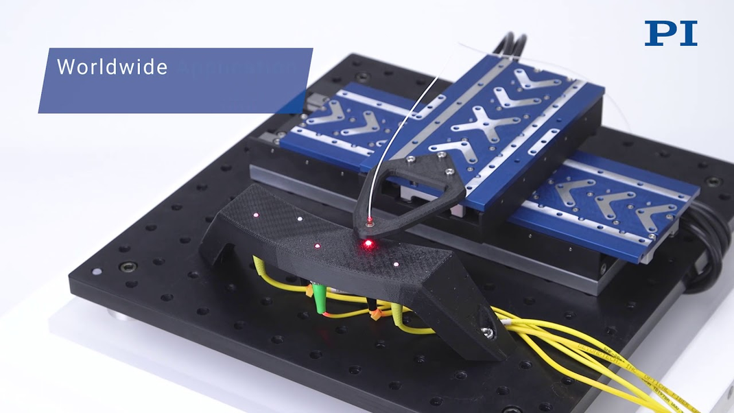
Sound familiar? That is the precise state of the photonics market today. And once again, we see a manufacturing ecosystem starting to emerge, propelled by pioneering entrants in the toolmaker, contract manufacturer, integrator, and industry consortium fields. There are even parallels to the groundbreaking technological innovations that animated the semiconductor toolmaker market, such as the introduction of the high performance two-armed robot capable of handling two wafers at once, heralding an era of rapidly rising manufacturing productivity. As always in manufacturing of highly precise components, advances in precision motion control drive progress. Already, the photonics circuit manufacturing-and-test arena’s first productivity revolution has burst disruptively onto the scene: 2016’s advent of Fast Multichannel Photonic Alignment (FMPA) technology from PI, capable of simultaneous optimization of multiple inputs, outputs, elements, and degrees-of-freedom.
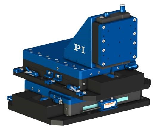
When space is a concern, a host of compact alignment solutions is available, using miniaturized stages with wear-free, high-speed linear motors, and high-precision crossed-roller guides, or – when the highest performance, cleanliness and lifetime is required – air bearings. The compact XYZ alignment stage unit above is based on an XY configuration of two A-142 air bearings slides and the V-308 voice coil linear slide with magnetic counterbalance for vertical mount.
By cutting alignment times by typically a factor of 100 for today's common photonic array devices, this addresses key production-economics challenges in applications as diverse as on-wafer chip test and assembling co-packaged optics and interconnects. Like the semiconductor industry’s first two-armed robot, FMPA parallel active alignment throws a vital focus on improving production metrics like cost-of-ownership and units-per-hour.
What follows is a snapshot of pioneers in key areas of service to the photonic-device manufacturing market. The field is churning, but the pioneers will always be the pioneers.
Consortia, Pilot Lines, Institutes
Industry consortia, pilot lines, and public-private institutes have emerged to illuminate the path toward scalable production of photonic devices. Europe, for example, enjoys a collection of photonic pilot lines (https://ec.europa.eu/programmes/horizon2020/en/news/more-photonic-pilot-lines-europe) focused on key device subtypes, such as InP-centered InPulse (https://www.jeppix.eu/jeppix-pilot-line/services/) and research-forward, packaging-technology-oriented PIXAPP (https://pixapp.eu). Across the Atlantic, the United States benefits from the AIM Photonics initiative, a broad-based endeavor facilitating the transition from research to manufacturing of integrated photonic devices (https://www.aimphotonics.com/about-us).
A new and important entrant is PODIUM (https://www.podiumpackaging.com), an industry consortium devoted to scalable packaging technologies for industry. PODIUM is a project under the Dutch funding organization PhotonDelta and is affiliated with the Chip Integration Technology Center (https://www.citc.org/program-lines/integrated-photonics-packaging/). PODIUM is composed of a synergistic cluster of members, including the aforementioned PHIX, PI, and Tegema. Uniquely, PODIUM bridges the gap between institute and OSAT, offering a nucleus of expertise in packaging process development. For this consultative, industrial-focused consortium, a key goal is to devise a path for scalable mass production for SiPh device designers. For example, PODIUM offers access to a low-cost, scalable platform for developing assembly strategies for SiPh devices and co-packaged optic assemblies. These can include optical fiber termination to photonic ICs and the necessary industrialization steps. PODIUM process development is founded on a modular platform approach that ensures scalability. PODIUM thus offers a ‘one stop shop’ from earliest packaging-process development all the way to production, with expert curation of technologies and suppliers to illuminate the make/buy decisions confronting photonic device developers. Sited near the heart of the Netherlands’ historically important photonics hub, PODIUM is internationally accessible and features participation by key high performance micro-assembly-automation experts.
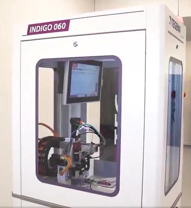
TEGEMA is a PODIUM member and offers the first commercially available high-throughput photonics packaging tools featuring PI’s FMPA technology. In TEGEMA’s tool, the parallel-alignment capabilities of FMPA are augmented by clever parallelism in handling, preparation, dispense, and cure sub-processes. The result is a ten times improvement in part throughput versus legacy approaches. A modular architecture was established to allow investment-preserving scalability that allows device manufacturers to transition from research phase to fully automatic, high-volume production. For example, parts handling can progress from operator loading to automated tray or conveyor loading by adding the necessary modules.
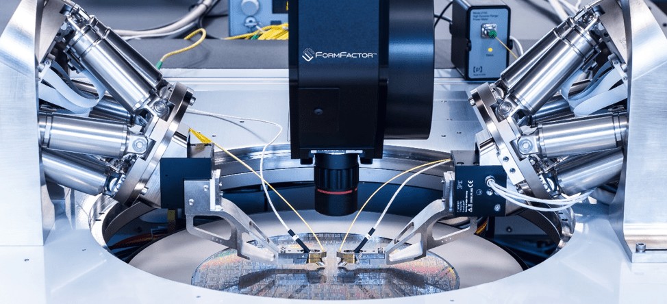
FormFactor offered the very first high-productivity tool for wafer-level silicon photonics test early in the Silicon Photonics era, with its advanced photonics engineering probers that implement FMPA parallel alignment capability on one or more sides of the chip under test, vastly improving productivity versus previously available engineering and even current production probers. Diffractive-coupler and edge-coupled connectivity is supported for wafers and singulated chips, with various options for handling automation. Since packaging costs dominate silicon photonic chips even more than with conventional microelectronic chips, it is even more imperative for only known-good chips to progress through to packaging. Because of this, probers are among the most important and numerous tools in a fab, as they validate the functionality of chips (preventing costly packaging operations from being attempted on a faulty chip), and they also enable binning, the practice of grading chips by performance for marketing into applications of different demands. The need for multiple probers to accommodate fab product flow makes their throughput even more critical.
Contract Manufacturers and OSATs
Many SiPh device manufacturers strategize their production by leveraging the expertise and resources of Outsourced Semiconductor Assembly and Test (OSAT) enterprises and specialized contract manufacturers.
For example, Integra Technologies is a fast-turnaround Silicon Valley fixture with capabilities across a wide range of chip test and packaging processes, including DMEA Accredited Category 1A Trusted applications involving highly sensitive tasks, and with facilities in Albuquerque and Wichita. Early in the Silicon Photonics saga, they pioneered custom SiPh change-kits: briefcase-sized personalization modules that accommodate each chip design’s I/O configuration within a multi-purpose high-speed tester tool, allowing one tool to be used for many types of chips. These bespoke photonic change-kits integrated PI’s FMPA fast photonic scan/align technology to accommodate high-speed validation of SiPh chips in various stages of assembly. At the time, the industry’s focus was on high-speed networking interconnect technologies for data centers. But as SiPh has broadened into consumer and other non-datacom applications, Integra-Tech kept pace. Recently, Integra-Tech branched out into contract assembly, implementing new cleanroom integration capabilities for exploring, developing, and scaling process approaches (https://www.integra-tech.com/blog/integra-technologies-expands-silicon-photonics-capabilities). Their first packaging venture involved just such a non-datacom chip: a phased array device similar to that described some years ago (https://www.researchgate.net/publication/304536829_Highly_integrated_optical_phased_arrays_Photonic_integrated_circuits_for_optical_beam_shaping_and_beam_steering) for shaping and laser beams steering for communications and LIDAR.
Benchmark Electronics has extensive capability in process-engineering and assembly of fiber optic and SiPh devices, including highly differentiating expertise in Liquid Crystal Polymer substrates (https://www.bench.com/photonics). This bleeding-edge substrate technology enables especially space-efficient designs with physical robustness and extraordinary speeds exceeding 110GHz. Benchmark's optical and photonic capabilities include a spectrum of manufacturing proficiency benefiting photonic integrated circuit packaging, termination, and hybrid module assembly. Their experience spans transceivers, pumps, tunable and fiber lasers, DWDM, OADM, router, line cards, and switches.With some of the biggest names in the field relying on Benchmark’s new Phoenix, Arizona RF and High Speed Design Center of Innovation for design and packaging services, Benchmark has recently developed an advanced, FMPA-based photonics automation architecture to continue its edge in productivity and quality. The new proprietary platform leverages the parallelism and industrial-class submicron motion qualities of PI’s architecture, ensuring extensibility and quick-response customization— essential capabilities for the rapidly-evolving photonics device market.
Custom Integrations
Finally, as noted in the introduction to this article, in the case of the early semiconductor industry, we saw custom tool development pursued for a long while as the ecosystem emerged. These efforts leveraged internal (captive) and external systems integration houses to design, assemble, and support production roll-out and expansion. As the toolmaker market matured, the need for custom integration lessened.
Custom design and integration are still the preferred course for many Silicon Photonics players and remains an entirely valid approach. Motivations for this include lack of standardization, lead-time concerns, proprietary application, and leveraging complementary organizational expertise.
Integration projects of this sort can benefit from the experience and connections of precision motion and positioning equipment suppliers, like PI. Recently, PI opened itsSilicon Valley Tech Center with a goal to provide a secure collaboration facility where subsystems work can be performed in cooperation with integration engineering teams, instrumentation manufacturers, and other external resources.
Conclusion
The field of Silicon Photonics has entered an exciting new phase as SiPh technology has broadened from data center into consumer, health, personal computing, and other new applications. SiPh device manufacturers can now access an expanding array of resources for getting devices to market with sustainable production economics.

